What is RF Frequency Synthesizer ?
The device used to select rf carrier frequency from pool of frequencies in wireless system is called RF synthesizer. It is used as variable RF frequency generator source. The tuning of RF frequency depends on the step size. It is responsible for generating stable and tunable RF signals at various frequencies.
It is used for various applications such as in RF transceiver, base stations, mobile subscribers, test and measurement equipments such as VSG (vector signal generator), VSA (vector signal analyzer) and so on. It's usage span across multiple technologies especially satellite communication, terrestrial microwave communication, wireless communication, radar etc.
Frequency synthesizer block diagram
RF frequency synthesizer typically consists of several components with Phase Locked Loop (PLL) and Voltage Controlled Oscillator (VCO) being key elements.
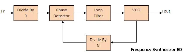
As shown in the frequency synthesizer block diagram,
PLL consists of reference frequency, Phase detector, Loop filter, frequency divider and
VCO.
The PLL is a closed-loop feedback system that compares the output frequency of the VCO with a reference frequency. It adjusts the control voltage applied to the VCO to minimize the phase difference between the two signals, thereby locking the output frequency to the reference frequency.
Frequency synthesizer output frequency is mathematically calculated using following equations as per its type.
1. Fout = N*(Fr/R) , for Integer PLL
2. Fout = (N+F)*(Fr/R), for fractional PLL
As mentioned here Output frequency of synthesizer is multiple of input frequency,
hence often frequency synthesizer is
called as frequency multiplier.
Output of frequency synthesizer can be obtained by either fixing Fr and varying N or
varying Fr and fixing N.
The RF synthesizer design example mentioned below is for the second case.
Channel spacing=Fvco/N or Fr/R.
Frequency synthesizer components functions/working
Let us understand functions of various components of frequency synthesizer.
• VCO: The VCO is responsible for producing an oscillating RF signal whose frequency can be varied by
applying a control voltage. The VCO's output frequency is directly related to the input control voltage.
• Phase Detector (PD) : As shown in RF synthesizer block diagram,
phase detector/comparator compares two input signals and
produces DC voltage(error voltage) based on phase difference of the two.
Phase detector can be considered as simple EX-OR gate.
• Loop filter : It is a simple Low Pass Filter, which removes high frequency noise and produces dc level.
• Frequency Dividers : The VCO output frequency is compared with the reference frequency and adjusted until it is equal to the
input frequency. Divide by R and Divide by N are simple frequency dividers.
Frequency dividers are used in synthesizer design to divide down the VCO output frequency to generate
the desired output frequency with better resolution.
• Control Interface : Provides a means for external control and programming of the synthesizer parameters, such as frequency and modulation
settings.
• Output Buffer/Amplifier : Amplifies and conditions the output signal for transmission or further processing.
PLL operates in three stages as mentioned below.
1. Free running: Before the input is applied to the PLL, PLL is said to be in free running state.
2. Capture: As soon as input frequency is applied, VCO frequency will start to change and PLL is said to be in
capture mode.
3. Phase Lock: VCO frequency continues to change till it is equal to the input reference frequency and
PLL in this condition is said to be in phase locked state.
Example of RF synthesizer design
Let us understand design of frequency synthesizer using PLL IC, DDS chip, VCO and
other components with following desired specifications.
• Output frequency: 950-1450 MHz
• Step size: 1 MHz
• Low Phase noise: -88 dBc at 1 KHz offset
• Spurious: -70dBc
• Harmonics: less than -20dBc typically
• External Reference: 10 MHz
Consider following rules of thumb during RF synthesizer design.
• Switching time approximately equals to 50/Fcomp, where Fcomp is the comparison frequency at the input of Phase comparator/detector.
• Switching time approx. equal to 2.5/Flbw, where Flbw is the loop bandwidth of loop filter.
• Loop filter loop bandwidth= 1/10 (Fcomp).

Following steps are followed during design.
➨As mentioned here the design of frequency synthesizer is done by buying out PLL chip, VCO chip and DDS chip.
We have selected, PLL chip as ADF-4252 from Analog devices, VCO as V585ME40 from ZCOMM and DDS chip as AD9851 from
Analog devices.
➨The loop filter need to be designed based on the rules of thumb mentioned above.
Loop filter design can be done by entering required parameters.
➨In the design of rf synthesizer various parameters are optimized based on requirement.
For example for the case where switching time is not so critical, then choice of loop
parameters will be determined by phase noise and spurious specifications.
Loop filter tools are available on the various websites such as https://www.ti.com/,
https://www.analog.com/ and www.circuitsage.com .
Conclusion : The RF frequency synthesizer design involves the integration of a Phase-Locked Loop (PLL) and a Voltage-Controlled Oscillator (VCO) to generate stable and tunable radio frequency signals. The synthesizer includes a control interface for user adjustments.
Similar posts on RF frequency synthesizer
Crystal oscillator vs frequency synthesizer
OCXO vs VCXO vs TCXO vs DCXO
Synthesizer manufacturers
PLL basics
What is DDS